808nm
808nm 5mW 3030 VCSEL SMD
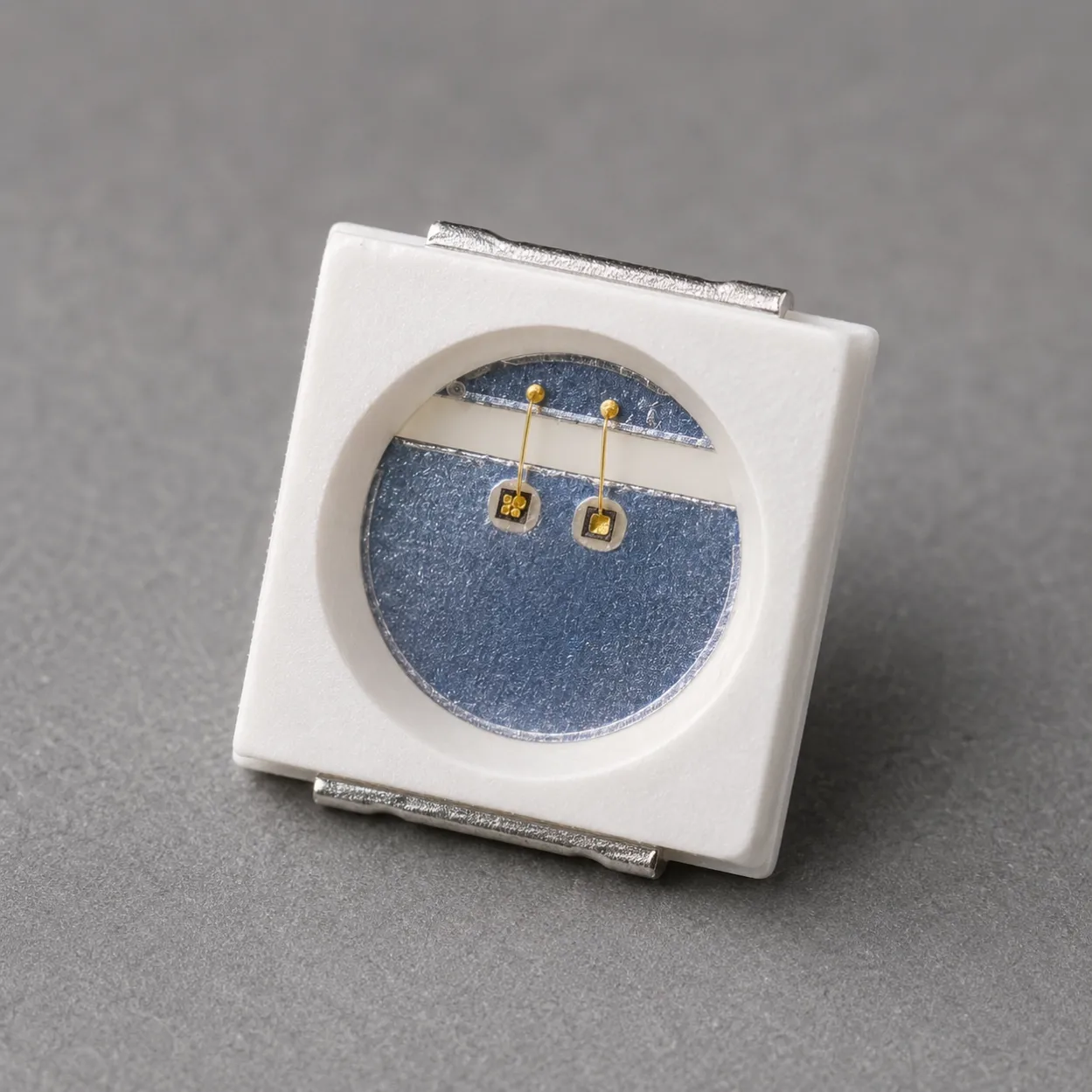
808nm 5mW 3030 VCSEL SMD with 5.5mW typical optical output, 21° typical D86 divergence and pulsed/QCW operation for compact PCB sensing projects.
Specifications
- Product Type
- VCSEL SMD
- Wavelength
- 808nm typ. (800–816nm)
- Optical Output Power
- 5.5mW typ.; 6mW max.
- Transverse Mode
- Multi-mode VCSEL
- Operating Mode
- Pulse / QCW
- Beam Divergence
- 21° typ. (18–24°)
- SMD Package Options
- 3030
1. 808nm 5mW 3030 VCSEL SMD for Low-Current PCB Optical Sources
The 808nm 5mW 3030 VCSEL SMD is a compact multimode near-infrared surface-mount laser source for low-current PCB sensing, optical detection, machine-vision support illumination and application-specific optical-module development.
At a forward current of 7mA, the device provides 5.5mW typical optical output and 6mW maximum optical output. Its peak wavelength is specified from 800nm to 816nm, with 808nm as the typical value. The typical beam divergence is 21° D86 within an 18° to 24° specified range.
The 3030 SMD package provides a nominal 3.0 × 3.0mm footprint and 0.6mm package height for compact surface-mount layouts. The product is intended for pulsed/QCW evaluation, with the actual drive waveform, duty cycle and thermal limits to be confirmed for the customer's operating condition.
This configuration is suited to projects that prioritize:
- A 7mA specified forward-current point
- Compact 3030 PCB integration
- 5.5mW typical 808nm optical output
- Automated SMT placement and reflow-process development
- Component-level sensing and measurement evaluation
- External lens, window or diffuser integration
Customers requiring chip-level die attach, wire bonding or custom packaging can compare the 808nm VCSEL Bare Die Series.
2. Optical and Electrical Characteristics
The principal optical and electrical characteristics of the 808nm 5mW 3030 VCSEL SMD are shown below.
Parameter | Minimum | Typical | Maximum | Test Condition |
|---|---|---|---|---|
Peak Wavelength | 800nm | 808nm | 816nm | 25°C |
Optical Output Power | — | 5.5mW | 6mW | IF = 7mA |
Threshold Current | — | 2mA | — | 25°C |
Forward Voltage | 1.8V | 2.0V | 2.2V | IF = 7mA |
Series Resistance | — | 75Ω | — | 25°C |
Slope Efficiency | — | 1W/A | — | 25°C |
Wavelength Temperature Coefficient | — | 0.047nm/°C | — | — |
Beam Divergence, D86 | 18° | 21° | 24° | D86 |
The 5.5mW typical and 6mW maximum optical-output values are specified at a forward current of 7mA. Pulse width, duty cycle and thermal limits should be defined for the customer's intended operating condition and verified during component evaluation.
For product selection and integration planning, this configuration uses a Multimode transverse mode and is intended for Pulsed/QCW operation. Because the optical-output row does not state a pulse width or duty cycle, confirm the project-specific drive condition before design release.
Performance in the completed PCB assembly can also be influenced by:
- Current-source stability
- Pulse waveform and duty cycle
- PCB trace resistance and parasitics
- Solder-joint quality
- Package temperature
- Optical-axis alignment
- External lens, diffuser or window transmission
The component should therefore be evaluated using the intended driver, PCB, optical structure and ambient conditions.
3. 3030 Package and SMT Integration
The device uses a compact 3030 surface-mount package for direct PCB placement and automated assembly.
Package Parameter | Specification |
|---|---|
Nominal Package Type | 3030 VCSEL SMD |
Nominal Package Length | 3.0mm |
Nominal Package Width | 3.0mm |
Nominal Package Height | 0.6mm |
Internal VCSEL Die Size | 7mil × 7mil |
Pin 1 | Cathode / negative |
Pin 2 | Anode / positive |
Tape-and-Reel Quantity | 4,000 pcs / reel |
The 3030 polarity is specific to this package: Pin 1 is cathode/negative and Pin 2 is anode/positive. It must not be replaced by the 2835 pin assignment used by the 10mW and 20mW products.
PCB and production development should verify:
- The recommended land pattern
- Package polarity before placement
- Solder-paste volume and stencil design
- Reflow profile for the selected PCB assembly
- ESD controls during storage and handling
- Optical clearance above the emitting area
- Lens or window position relative to the optical axis
- Local PCB thermal path under pulsed/QCW operation
The nominal package dimensions support compact board layouts, but final footprint, process and enclosure decisions should be checked against the corresponding package drawing and production conditions.
4. Application Development
The 808nm 5mW 3030 VCSEL SMD is positioned as the lowest-current member of the 808nm SMD group. It provides a completed surface-mount source for projects that need compact PCB placement and a 5.5mW typical optical-output level.
Compact Sensing and Detection Modules
The 7mA specified current point and 3030 footprint can support evaluation in compact near-infrared sensing and detection modules where PCB area, driver current and optical alignment are important design inputs.
Possible component-level development directions include:
- Photoelectric sensing
- Object and presence detection
- Position and proximity sensing
- Reflective measurement
- Optical alignment systems
- Compact sensor-light-source boards
Detector responsivity, target reflectivity, ambient light, working distance and external optics must be evaluated in the complete system. The VCSEL optical-output value alone does not establish detection distance or finished-system performance.
Machine-Vision Support and Optical Measurement
The 808nm wavelength and compact surface-mount format can also support engineering evaluation for machine-vision support illumination, optical measurement and alignment equipment.
The 18° to 24° D86 beam-divergence range describes the component output before downstream optics. The final illuminated field depends on package alignment, lens or diffuser design, working distance and the mechanical stack-up.
This application description represents component-level development possibilities. It does not establish the safety classification, regulatory status or performance of the customer's finished equipment.
5. Evaluation Kit and Documentation Support
Evaluation samples can be discussed for low-current driver testing, 3030 PCB-footprint verification, SMT assembly trials, optical alignment and initial sensing-module integration. An Evaluation Kit with 10 pcs / KIT is available for PCB-layout verification, driver testing, pulse-control evaluation, soldering-process development, optical alignment and initial system integration.
Evaluation can support:
- 7mA drive-point verification
- Pulsed/QCW waveform evaluation
- 3030 land-pattern and polarity review
- SMT placement and reflow-process validation
- ESD-handling process review
- 21° typical D86 beam-divergence evaluation
- Lens, window or diffuser selection
- Compact PCB sensing-source development
Project-specific requirements can include wavelength tolerance, optical-output selection, drive conditions, package supply, downstream optics and volume-production planning.
For component-level project evaluation, an Initial Product Report covering the Laser Diode Series and VCSEL Laser Diode Chip Series has been filed with the U.S. FDA CDRH. This filing supports technical documentation and product evaluation.
For applicable products, CE, EMC, EN 60825, LVD, RoHS, REACH and halogen-free certification and compliance documents are available. Documentation depends on the corresponding product model and does not represent certification of the customer's finished device.
6. Frequently Asked Questions
FAQ 1. What are the main specifications of the 808nm 5mW 3030 VCSEL SMD?
The product has an 800nm to 816nm specified peak-wavelength range with 808nm as the typical value. At IF = 7mA, it provides 5.5mW typical and 6mW maximum optical output.
Its typical threshold current is 2mA, typical forward voltage is 2.0V and typical beam divergence is 21° D86 within an 18° to 24° specified range.
The optical-output row is specified at IF = 7mA without a stated pulse width or duty cycle. The intended Pulsed/QCW operating mode should therefore be evaluated under a confirmed project-specific drive condition.
FAQ 2. What polarity and PCB details apply to the 808nm 5mW 3030 package?
The nominal package size is 3.0 × 3.0mm with a nominal height of 0.6mm. For this 3030 package, Pin 1 is cathode/negative and Pin 2 is anode/positive.
PCB development should verify the corresponding land pattern, polarity, optical-axis position, solder-paste design, reflow profile, ESD controls and local thermal path. The 3030 pin assignment must not be assumed to match the 2835 products.
FAQ 3. When should I select the 5mW 3030 model instead of the 10mW or 20mW 2835 models?
Select the 5mW 3030 configuration when the project prioritizes the 7mA specified drive point, a compact 3030 footprint and 5.5mW typical optical output.
The 808nm 10mW 2835 VCSEL SMD and 808nm 20mW 2835 VCSEL SMD provide higher optical-output classes at 15mA and 28mA respectively under their specified test conditions. Final selection should consider required optical output, PCB footprint, current-driver capability, pulse condition, detector sensitivity, thermal design and downstream optics.