
670nm
670nm 4/9/12mW VCSEL Bare Die Series
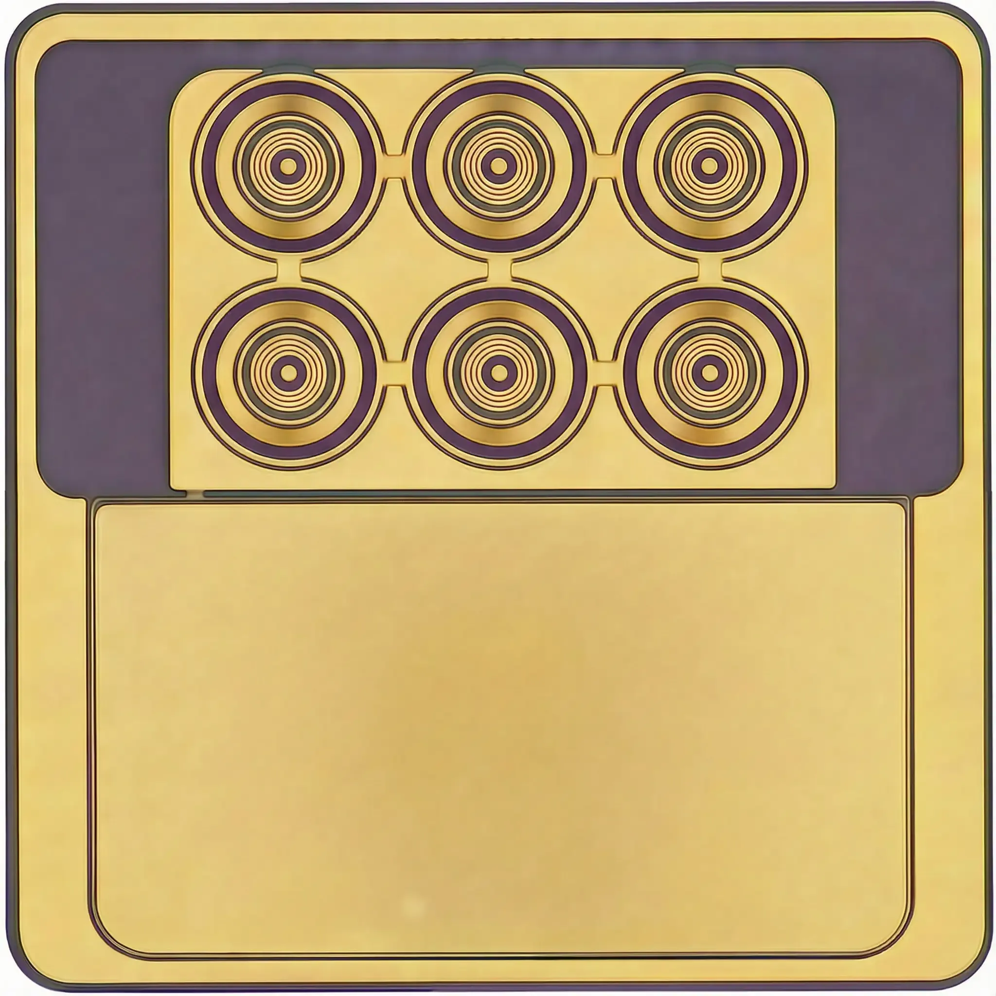
670nm 4mW, 9mW and 12mW VCSEL bare dies for wire bonding, ceramic-submount assembly, custom laser packaging and OEM red optical-source development.
Specifications
- Product Type
- Multi-mode VCSEL Bare Die
- Wavelength
- 670 nm typ.
- Optical Output Power
- 4mW / 9mW / 12mW class
- Emitter Configuration
- 1 / 4 / 6 Emitters
- Operating Mode
- QCW, 0.5ms Pulse Width, 1% Duty Cycle
- Die Size
- 200μm × 200μm / 170±10μm × 170±10μm / 163±10μm × 185±10μm
- Recommended Assembly
- Die Attach / Wire Bonding / Ceramic Submount / Custom Packaging
1. 670nm VCSEL Bare Die Series for Packaging and Module Development
The 670nm 4mW, 9mW and 12mW VCSEL Bare Die Series provides multi-mode visible-red chip options for die attach, wire bonding, ceramic-submount assembly and custom laser-source development. Under the source-specified QCW conditions, the three models provide 3.0-4.0mW at 10mA, 7.0-9.0mW at 18mA and 9.0-12.0mW at 25mA, respectively.
These are unpackaged semiconductor components. Package selection, mounting, bonding, thermal design, optics, eye safety and final device performance remain engineering responsibilities of the integrator.
2. 4mW, 9mW and 12mW Configuration Selection
670nm 4mW VCSEL Bare Die
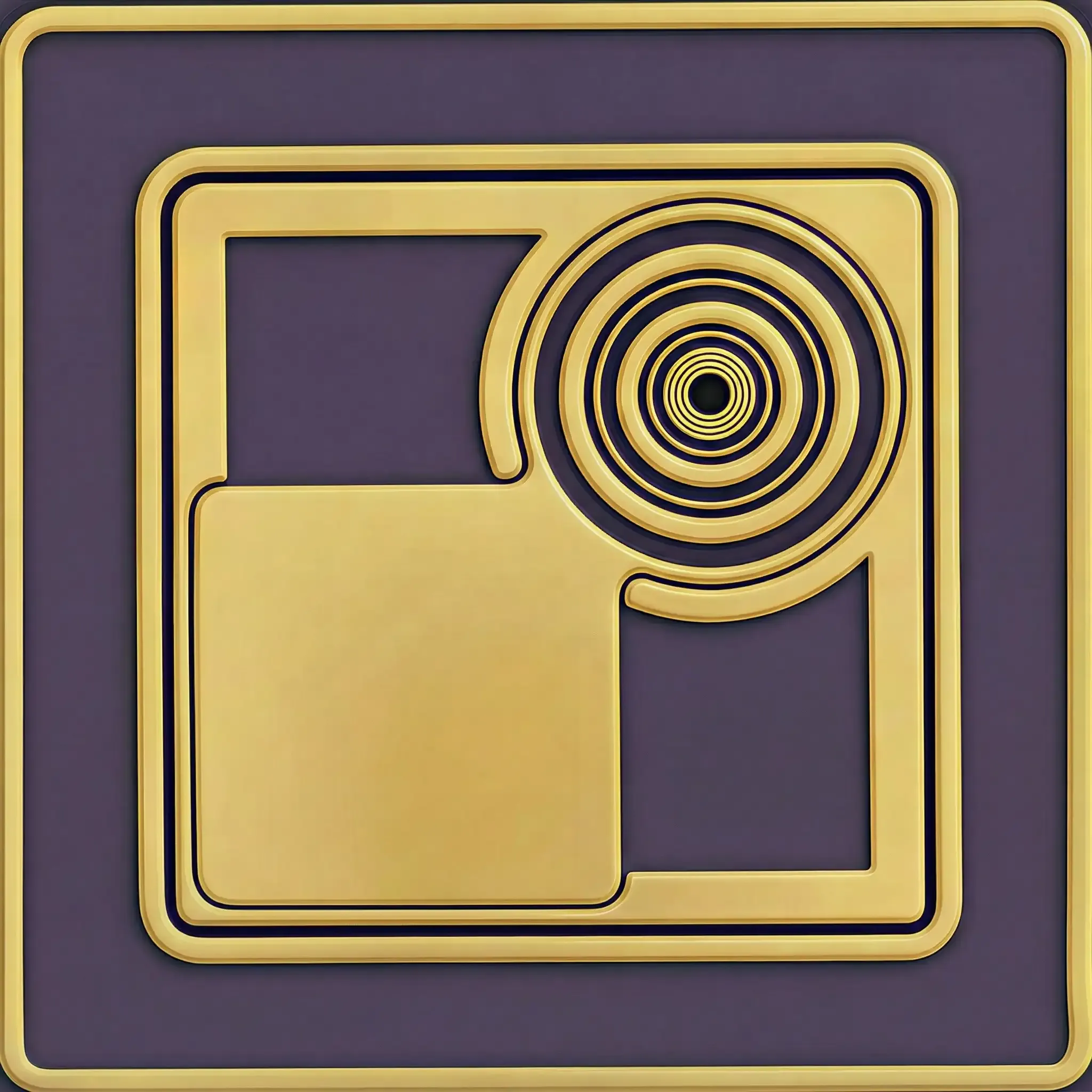
The 4mW model is a one-emitter die with 3.0mW minimum and 4.0mW typical optical output at 10mA, 25°C QCW. The source lists 668-670nm wavelength, 22° typical divergence and a 200μm x 200μm die size.
670nm 9mW VCSEL Bare Die
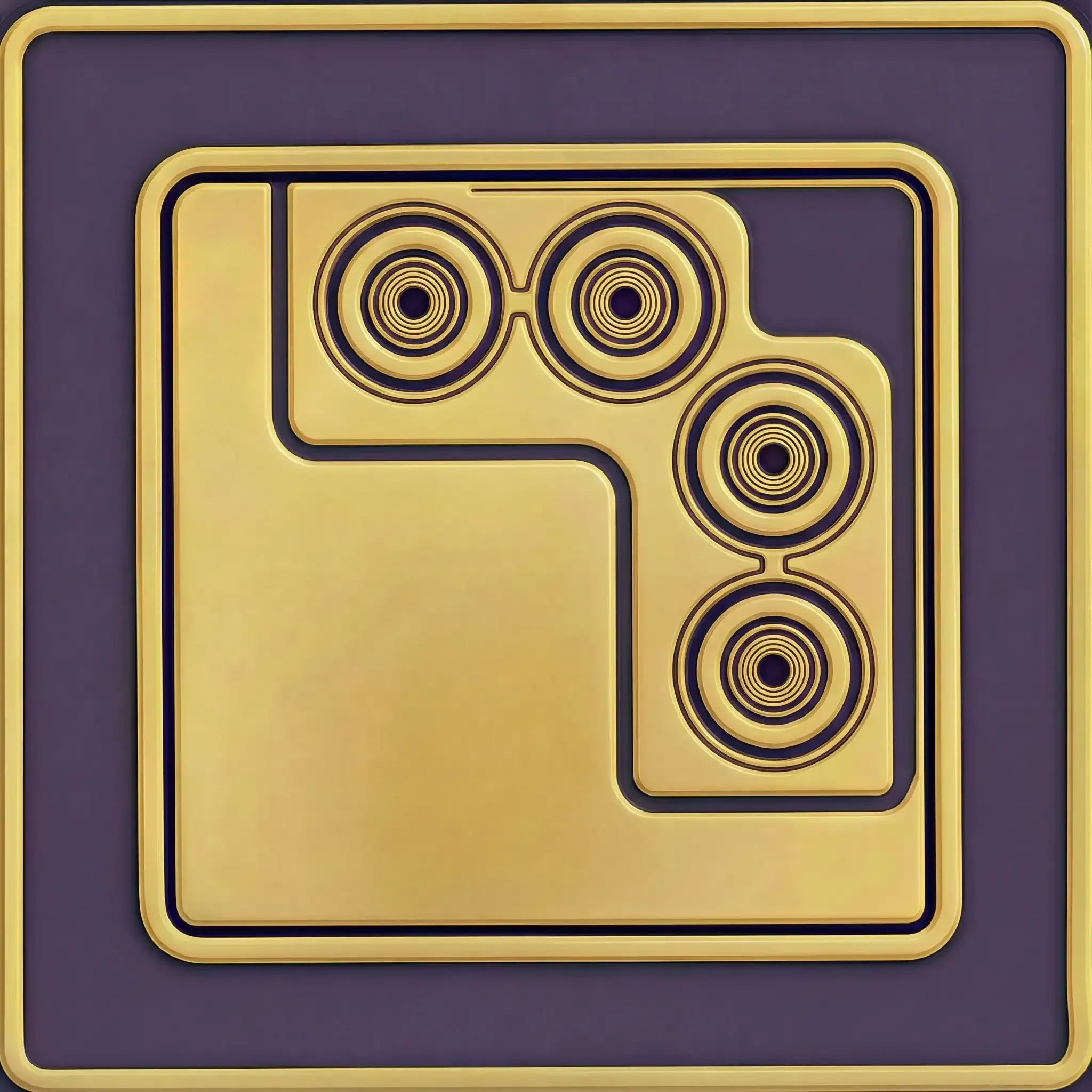
The 9mW model uses four emitters and lists 7.0mW minimum and 9.0mW typical optical output at 18mA, 25°C QCW. The source lists 667-670nm wavelength, 23° typical divergence and a 170±10μm x 170±10μm die size.
670nm 12mW VCSEL Bare Die
The 12mW model uses six emitters and lists 9.0mW minimum and 12.0mW typical optical output at 25mA, 25°C QCW. The source lists 667-670nm wavelength, 23° typical divergence and a 163±10μm x 185±10μm die size.
3. Annular Far-Field and Bare-Die Integration Considerations
The source data describes a symmetric donut-shaped far-field profile for this series. Optical performance in a finished assembly depends on the selected lens, collimation or beam-shaping approach, emitter configuration, mounting alignment, drive conditions and thermal path.
Use the individual product page when a project requires one source-specific configuration and test condition.
4. Evaluation Kit, Documentation and Custom Development Support
For early-stage bare-die assembly and optical evaluation, a 10 pcs / KIT evaluation quantity can be requested after the required output level and operating condition are defined.
For die selection, bonding-pad assessment, ceramic-submount design, package configuration or optical-source development, submit the application conditions and target operating parameters for engineering review.
For component-level project evaluation, an Initial Product Report covering the Laser Diode Series and VCSEL Laser Diode Chip Series has been filed with the U.S. FDA CDRH. This filing supports technical documentation and product evaluation.
For applicable products, CE, EMC, EN 60825, LVD, RoHS, REACH and halogen-free certification and compliance documents are available. Documentation depends on the corresponding product model and does not represent certification of the customer's finished device.
5. Frequently Asked Questions
FAQ 1. How should I choose between the 4mW, 9mW and 12mW models?
Start with the source-specified output range, drive current, emitter count, die size and optical integration target. The correct option must then be validated in the intended package and optical architecture.
FAQ 2. What assembly methods are appropriate for this bare-die series?
The product specifications identify die attach, wire bonding, ceramic submount and custom packaging as recommended assembly directions. The final process must be qualified by the integrator.
FAQ 3. Does the listed beam profile guarantee a finished-module beam shape?
No. The datasheet describes the source far field. The finished beam depends on the lens, alignment, package, drive, thermal path and the complete optical system.