670nm
670nm 12mW VCSEL Bare Die
670nm 12mW VCSEL bare die with six emitters, 12mW typical QCW output at 25mA and rectangular die geometry for red-light optical-module integration.
Specifications
- Product Type
- VCSEL Bare Die
- Wavelength
- 670 nm typ.
- Optical Output Power
- 12mW class, 9.0mW min. / 12mW typ. @ IF = 25mA
- Emitter Configuration
- 6 Emitters
- Operating Mode
- QCW, 0.5ms Pulse Width, 1% Duty Cycle at 25°C
- Die Size
- 163±10μm × 185±10μm
- Recommended Assembly
- Die Attach / Wire Bonding / Ceramic Submount / Custom Packaging
1. 670nm 12mW VCSEL Bare Die for Packaging and Module Integration
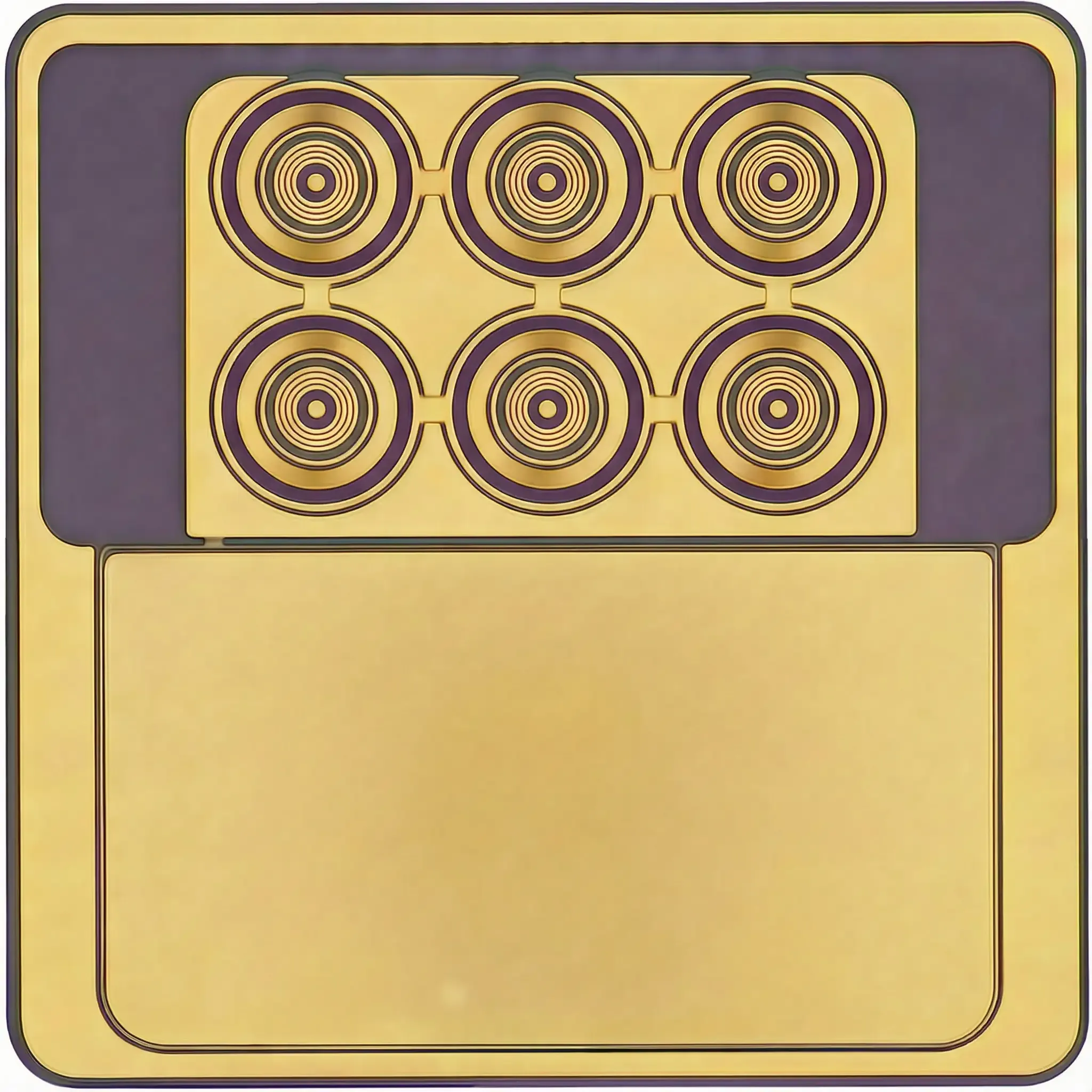
The 670nm 12mW VCSEL Bare Die is a six-emitter visible-red VCSEL chip designed for die attach, wire bonding and customer-defined laser packaging. It gives integration teams a higher-output option within the 670nm bare-die family while keeping the component boundary clear: the product is supplied as a die, not as a finished optical module.
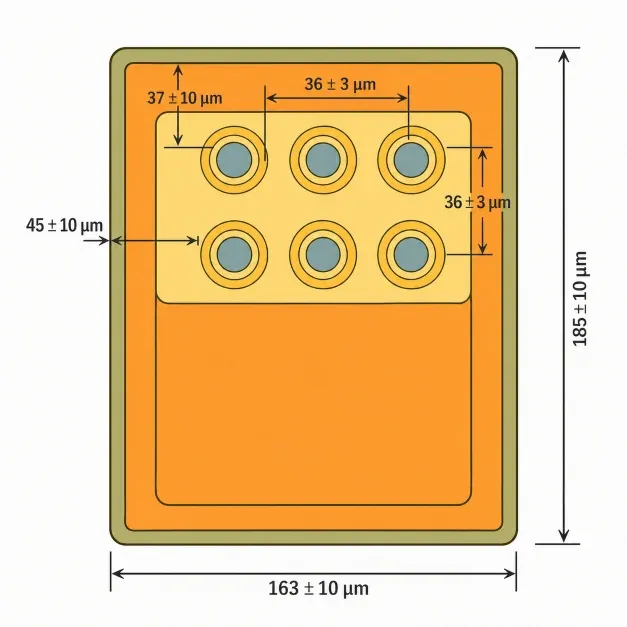
Under the datasheet QCW test condition at 25°C, with 0.5ms pulse width and 1% duty cycle, the component delivers 9.0mW minimum and 12mW typical optical output at 25mA. Its 163±10μm × 185±10μm rectangular die contains six emitters and uses a 115±3μm × 85±3μm bond pad, creating a distinct package-layout requirement from the square four-emitter 9mW version.
Development directions include:
- Six-emitter 670nm VCSEL packaging for laser-component manufacturers
- Rectangular-die placement, wire-bonding and ceramic-submount process development
- Component-level red-light source integration for optical modules
- Sensor-light, machine-vision and consumer-electronics source evaluation
- Higher-output selection within a coordinated 670nm bare-die product family
The package designer remains responsible for mechanical protection, electrical connection, heat flow and optical coupling. Optical output stated here is measured under the datasheet condition; it is not a promise of finished-module power, power density or system performance.
2. Optical Configuration and Packaging Direction
The six-emitter layout, rectangular outline and 25mA test point distinguish the 670nm 12mW VCSEL Bare Die. Use the following datasheet values when screening the device for package, driver and optical-design compatibility.
Parameter | Datasheet Value |
|---|---|
Optical Output Power | 9.0mW min. / 12mW typ. @ IF = 25mA |
Wavelength | 667nm min. / 670nm typ. |
Threshold Current | 7.5mA typ. |
Forward Voltage | 2.6V typ. @ IF = 25mA |
Slope Efficiency | 0.6W/A typ. |
Power Conversion Efficiency | 16% typ. @ IF = 25mA |
Beam Divergence | 23° typ. at 1/e² and IF = 25mA |
Operating Condition | QCW, 0.5ms pulse width, 1% duty cycle at 25°C |
Emitter Configuration | 6 emitters |
Die Size | 163±10μm × 185±10μm |
Die Thickness | 130±10μm |
Bond Pad Size | 115±3μm × 85±3μm |
Backside Cathode Size | 163±10μm × 185±10μm |
This model is appropriate when a project specifically needs the documented 12mW typical output, six-emitter architecture and rectangular die geometry. The 25mA value is the datasheet characterization point under the stated QCW condition, not an unrestricted recommendation for a customer-designed package.
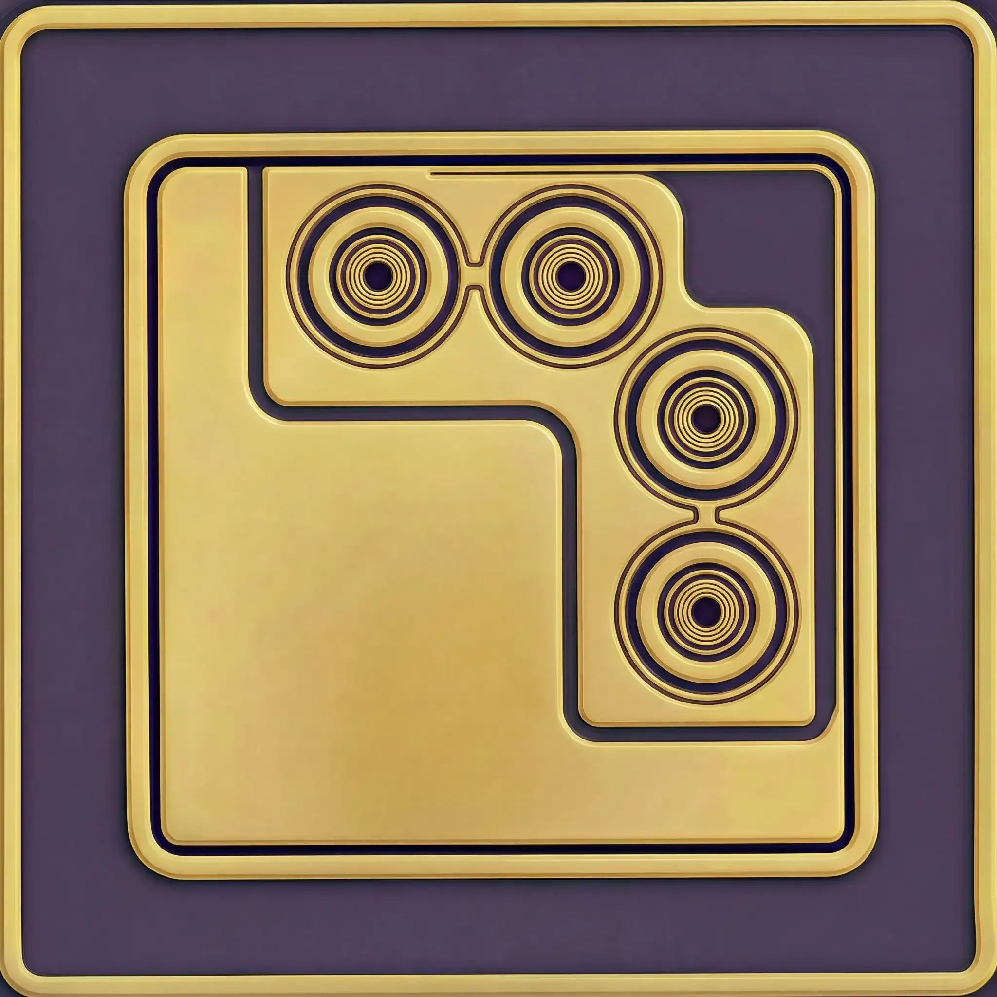
For a lower-output four-emitter component with a square 170±10μm × 170±10μm outline and 9mW typical output at 18mA, compare the 670nm 9mW VCSEL Bare Die. Electrical, thermal and optical qualification is required before substituting either die in an existing assembly.
3. Packaging, Optical Module and Application Development
OSAT and Custom Laser Packaging
The 12mW component needs a package layout matched to its six-emitter structure and rectangular dimensions. OSAT and in-house packaging reviews should address:
- Orientation and placement controls for a 163μm × 185μm-class die
- Die-attach material, process window and bond-line consistency
- Wire-bond tool access to the 115±3μm × 85±3μm pad
- Ceramic-submount routing, electrical return and heat-flow design
- Protective TO-can or custom-package development
- ESD handling, inspection criteria and packaged-sample qualification
Its wider bond pad and non-square outline should be reflected in tooling, substrate and package drawings. Process settings and thermal limits are integration decisions and must be validated through assembly trials rather than inferred from the optical table.
Lens and Optical Module Integration
The datasheet reports 23° typical beam divergence at 1/e² and 25mA. Optical engineers can use that stated test value as an initial input for package-to-lens spacing, collimator selection and beam-shaping studies, while recognizing that the completed package and drive condition can alter measured behavior.
Packaged samples should be characterized for optical power, power density, working distance, beam distribution, temperature response and mechanical alignment. These module-level results determine whether the source and optics satisfy the downstream design.
Downstream Application Development
According to the source datasheet, potential directions include sensor light sources, consumer electronic products, machine vision and red lighting. The 12mW six-emitter die can therefore be considered when a component-level project needs more output than the adjacent 9mW configuration and can accommodate its different geometry and current point.
Any PBM, personal-care or hair-growth reference is limited to component and module development. It does not claim therapeutic effect, clinical performance, regulatory clearance or approval of a finished customer device.
4. Evaluation Kit and Documentation Support
An Evaluation Kit can be discussed for early die-attach, wire-bonding, packaged-source and optical-coupling trials with the 670nm 12mW VCSEL Bare Die. For a useful technical review, provide the target package, proposed QCW drive, thermal concept, lens arrangement and measurement plan.
- 10 pcs / KIT
- Product datasheet and die-dimension documentation
- Technical review of six-emitter layout, output condition and package geometry
- International shipping quoted according to destination
For component-level project evaluation, an Initial Product Report covering the Laser Diode Series and VCSEL Laser Diode Chip Series has been filed with the U.S. FDA CDRH. This filing supports technical documentation and product evaluation.
For applicable products, CE, EMC, EN 60825, LVD, RoHS, REACH and halogen-free certification and compliance documents are available. Documentation depends on the corresponding product model and does not represent certification of the customer's finished device.
5. Frequently Asked Questions
FAQ 1. What makes the 670nm 12mW VCSEL Bare Die different from the 9mW product?
The 12mW product uses six emitters in a 163±10μm × 185±10μm rectangular die and is characterized at 25mA. The 9mW product uses four emitters in a 170±10μm × 170±10μm square die and is characterized at 18mA.
Those differences affect footprint, bond-pad access, driver design, thermal behavior and optical output. Selection should be based on the planned package and measured module requirements, not only on the nominal power label.
FAQ 2. Which conditions define the 12mW optical output and 23° beam value?
The datasheet specifies 9.0mW minimum and 12mW typical optical output at 25mA under QCW operation at 25°C, using 0.5ms pulse width and 1% duty cycle. It also states 23° typical beam divergence at 1/e² and 25mA.
These values belong to the documented component test condition. A packaged module must be retested with its actual driver, thermal path, optical stack and mechanical tolerances.
FAQ 3. What package changes should be checked for this six-emitter rectangular 670nm VCSEL die?
Check the substrate land pattern, die orientation, attach footprint, 115±3μm × 85±3μm bond-pad access, wire-loop clearance and the heat path beneath the 163±10μm × 185±10μm die. Tooling and inspection criteria should be designed for the rectangular outline rather than copied from a square-die process.
The assembled source should then be evaluated for optical output, power density, beam distribution, wavelength, temperature behavior and lens alignment under the intended pulse condition.