670nm
670nm 9mW VCSEL Bare Die
670nm 9mW VCSEL bare die with four emitters and 9mW typical QCW output at 18mA for square-die red-light source packaging and optical-module integration.
Specifications
- Product Type
- VCSEL Bare Die
- Wavelength
- 670 nm typ.
- Optical Output Power
- 9mW class, 7.0mW min. / 9.0mW typ. @ IF = 18mA
- Emitter Configuration
- 4 Emitters
- Operating Mode
- QCW, 0.5ms Pulse Width, 1% Duty Cycle at 25°C
- Die Size
- 170±10μm × 170±10μm
- Recommended Assembly
- Die Attach / Wire Bonding / Ceramic Submount / Custom Packaging
1. 670nm 9mW VCSEL Bare Die for Packaging and Module Integration
The 670nm 9mW VCSEL Bare Die is a four-emitter visible-red VCSEL chip for die attach, wire bonding, ceramic-submount assembly and custom laser packaging. It is intended for component and module teams that need a 9mW-class 670nm source in bare-die form rather than a finished laser package.
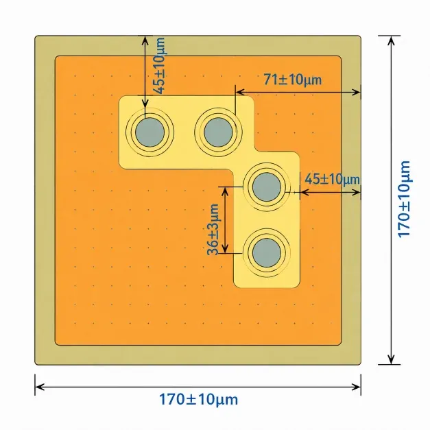
At 25°C under the datasheet QCW condition of 0.5ms pulse width and 1% duty cycle, the device provides 7.0mW minimum and 9.0mW typical optical output at 18mA. Its 170±10μm × 170±10μm square die contains four emitters, with an 87±3μm × 85±3μm bond pad documented for package-layout and bonding-process evaluation.
This configuration is relevant to:
- OSAT teams developing a process for a 170μm-class square VCSEL die
- Laser-component manufacturers evaluating four-emitter 670nm red VCSEL packaging
- Optical-module engineers building component-level red-light or sensor light sources
- Machine-vision and consumer-electronics teams qualifying a packaged 670nm source
- Sourcing teams comparing output and geometry options within the 670nm bare-die family
This is an unpackaged semiconductor die. The customer must design and validate die attach, electrical interconnection, thermal management, protective packaging and downstream optics. Datasheet values describe the component under stated test conditions and do not guarantee the performance of a finished module.
2. Optical Configuration and Packaging Direction
The 670nm 9mW VCSEL Bare Die combines four emitters with a square die outline and an 18mA datasheet test point. The following selection-critical values come from the current product datasheet.
Parameter | Datasheet Value |
|---|---|
Optical Output Power | 7.0mW min. / 9.0mW typ. @ IF = 18mA |
Wavelength | 667nm min. / 670nm typ. |
Threshold Current | 4.6mA typ. |
Forward Voltage | 2.7V typ. @ IF = 18mA |
Slope Efficiency | 0.6W/A typ. |
Power Conversion Efficiency | 16% typ. @ IF = 18mA |
Operating Condition | QCW, 0.5ms pulse width, 1% duty cycle at 25°C |
Emitter Configuration | 4 emitters |
Die Size | 170±10μm × 170±10μm |
Die Thickness | 130±10μm |
Bond Pad Size | 87±3μm × 85±3μm |
Backside Cathode Size | 170±10μm × 170±10μm |
The 9mW model is the square-die, four-emitter choice when the documented 18mA QCW operating point and 170μm-class outline suit the package concept. Drive current, pulse conditions and optical output must be verified in the intended assembly; the datasheet test point is not a universal drive recommendation for every module.
For a six-emitter configuration with 12mW typical optical output at 25mA and a rectangular die outline, review the 670nm 12mW VCSEL Bare Die. Its electrical point, geometry and bonding layout differ, so it should be qualified as a separate component rather than treated as a drop-in replacement.
3. Packaging, Optical Module and Application Development
OSAT and Custom Laser Packaging
The four-emitter layout, square die geometry and documented electrode dimensions provide a basis for package-process planning. Relevant engineering work can include:
- Die orientation, placement and attach-process development
- Gold-wire bonding and bond-loop evaluation
- Ceramic-submount routing and pad-access planning
- TO-can or application-specific laser-package development
- Thermal-path, package-material and ESD-control verification
- Incoming inspection and alternative-source qualification
The 87±3μm × 85±3μm bond pad and square backside cathode define the starting geometry for bonding-tool access and submount design. Attach material, bonding parameters, package protection and thermal limits must be established and qualified by the integration team.
Lens and Optical Module Integration
After packaging, the four-emitter 670nm die can be paired with application-specific collimation, diffusion or beam-shaping optics. Optical development should define source position, package-to-lens tolerance, working distance and the target distribution of optical power.
Final beam shape, optical power, power density and uniformity depend on the packaged source, drive condition, temperature and downstream optics. Those characteristics must be measured in the customer's assembled module and must not be inferred from bare-die dimensions alone.
Downstream Application Development
The source datasheet identifies sensor light sources, consumer electronic products, machine vision and red lighting as application directions. For these projects, the 670nm 9mW VCSEL Bare Die is a component-level optical source that requires packaging and system qualification before use.
PBM, beauty or hair-growth projects may evaluate this die only as a visible-red component for package and optical-module development. These application possibilities do not represent medical efficacy, clinical performance, therapeutic claims, regulatory approval or certification of the customer's finished device.
4. Evaluation Kit and Documentation Support
The 670nm 9mW VCSEL Bare Die can be discussed for an Evaluation Kit supporting die-attach trials, wire-bonding verification and initial packaged-source measurements. The request should identify the intended package, pulse condition, optical arrangement and evaluation objective.
- 10 pcs / KIT
- Product datasheet and die-dimension documentation
- Review of wavelength, output, emitter layout and package-integration requirements
- International shipping quoted according to destination
For component-level project evaluation, an Initial Product Report covering the Laser Diode Series and VCSEL Laser Diode Chip Series has been filed with the U.S. FDA CDRH. This filing supports technical documentation and product evaluation.
For applicable products, CE, EMC, EN 60825, LVD, RoHS, REACH and halogen-free certification and compliance documents are available. Documentation depends on the corresponding product model and does not represent certification of the customer's finished device.
5. Frequently Asked Questions
FAQ 1. What output, emitter count and die geometry define the 670nm 9mW VCSEL Bare Die?
The datasheet specifies 7.0mW minimum and 9.0mW typical optical output at 18mA under a 25°C QCW condition with 0.5ms pulse width and 1% duty cycle. The component uses four emitters in a 170±10μm × 170±10μm square die with 130±10μm thickness.
These are bare-die characteristics under the stated test condition. Output from a packaged optical module also depends on assembly quality, drive electronics, thermal behavior and optical losses.
FAQ 2. When should a project select the 9mW four-emitter die instead of the 670nm 12mW option?
Select the 9mW version when the project needs the documented 18mA operating point, four emitters and a 170μm-class square die. The 12mW sibling is characterized at 25mA, uses six emitters and has a 163±10μm × 185±10μm rectangular outline.
The decision should follow package footprint, bond-pad access, driver capability, thermal path, required optical output and module-level test results. The two products should not be treated as interchangeable without qualification.
FAQ 3. What should an OSAT evaluate when packaging this 670nm 9mW square VCSEL die?
The process plan should cover die orientation, placement accuracy, attach material, cure or reflow profile, wire material, bond-loop geometry, ESD handling, submount routing, heat flow and package cleanliness. Bond-pad access should be checked against the documented 87±3μm × 85±3μm geometry.
After assembly, the team should verify wavelength, packaged optical output, power density, temperature behavior and compatibility with the selected lens system under the intended pulse condition.