
Jun 15, 2026Application Insights
VCSEL Applications: How Vertical-Cavity Lasers Power Sensing, LiDAR and Data Links
Explore how VCSEL technology supports 3D sensing, LiDAR, data communication, industrial measurement, and custom OEM optical systems.
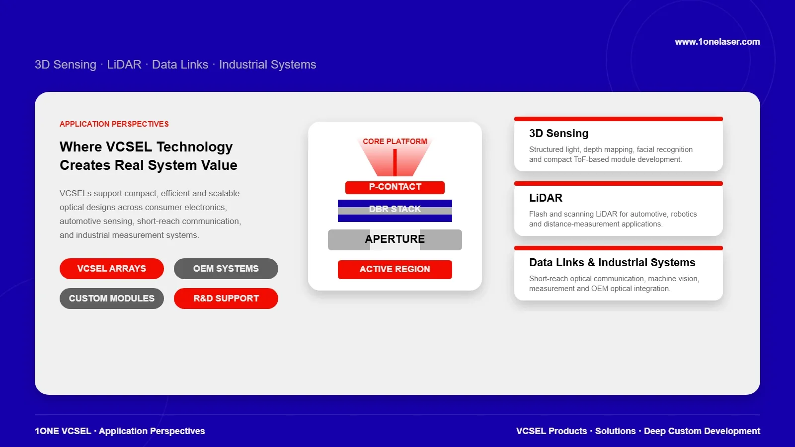
A vertical-cavity surface-emitting laser, better known as a VCSEL, has moved far beyond its original role as a specialized semiconductor laser. Today, it serves as an optical source in structured-light systems, time-of-flight sensors, LiDAR, short-reach communication, machine vision, medical beauty devices, quantum sensing platforms, and high-power near-infrared modules.
What makes a VCSEL suitable for a project is not just its wavelength or headline optical power. Device structure, emission direction, array layout, pulse conditions, package, thermal path, beam divergence, and receiver design all influence the final result.
This application-focused guide explains how VCSEL technology works, where it is used, and what R&D teams, testing laboratories, and OEM engineers should consider before choosing a standard component or moving toward a deeper custom solution.
What Is a VCSEL?
VCSEL stands for vertical-cavity surface-emitting laser.
The most obvious difference between a VCSEL and an edge-emitting laser is the direction of the optical output.
An edge-emitting laser sends light through the side of the chip, with the optical cavity running parallel to the wafer surface. A VCSEL sends light vertically through the top or bottom of the semiconductor stack.
That structural difference creates several practical advantages:
- Wafer-level electrical and optical testing
- Straightforward integration into one-dimensional or two-dimensional arrays
- Compact alignment with lenses, diffusers, fibers, and diffractive optical elements
- Small optical module footprints
- Scalable emitting area and total optical power
- Fast modulation and short-pulse operation
A single-emitter VCSEL may be suitable for a focused optical source or moderate output level. A VCSEL array is often selected when the system needs more total power, broader illumination, or a defined emitter pattern.
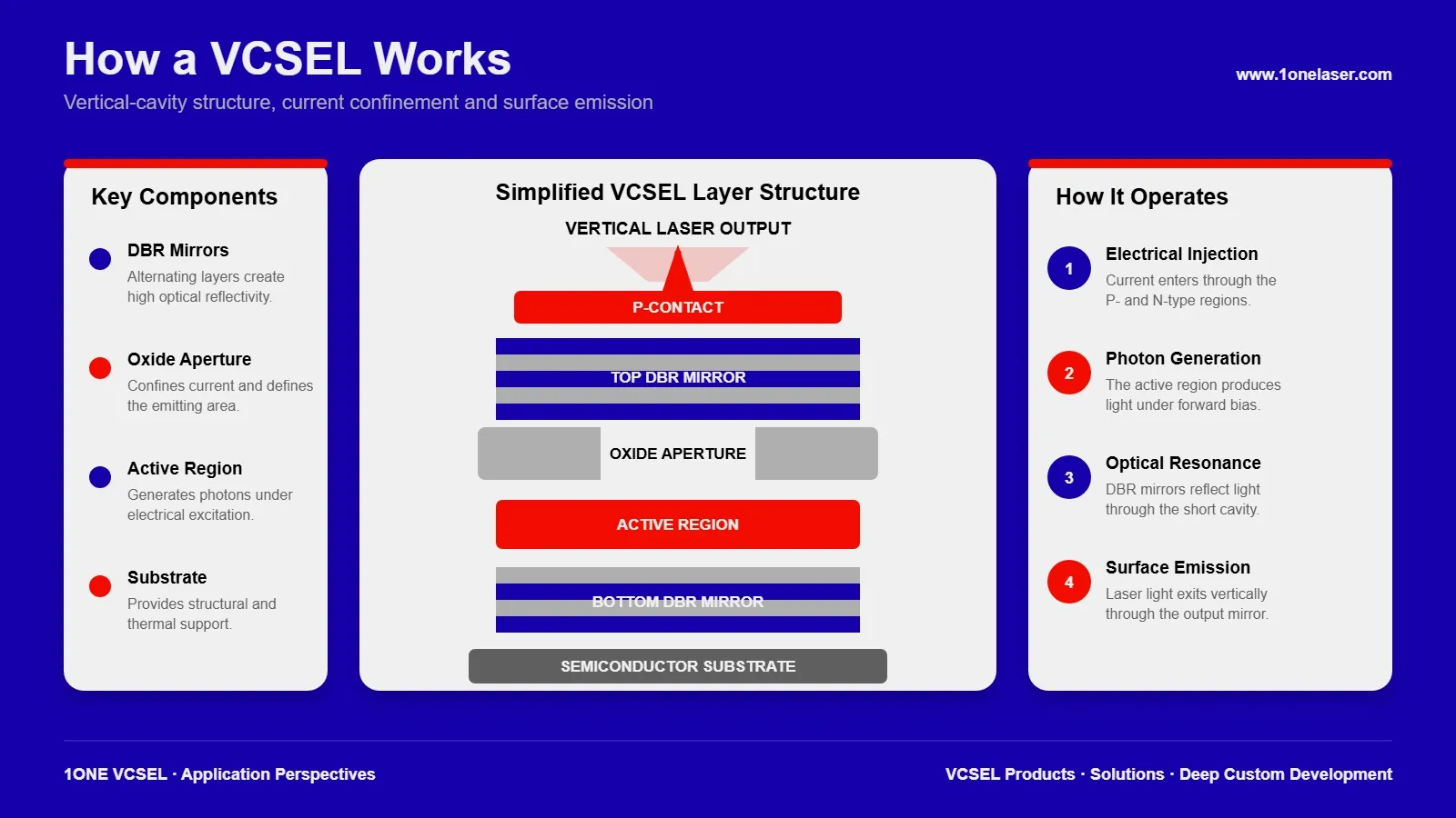
How Does a VCSEL Work?
A typical VCSEL includes an active region, two distributed Bragg reflector stacks, a current-confinement structure, electrical contacts, and a semiconductor substrate.
Active Region
The active region is where photons are generated.
When current passes through the semiconductor junction, electrons and holes recombine and produce light. The material system and quantum-well design influence the center wavelength, efficiency, temperature behavior, and modulation performance.
Distributed Bragg Reflectors
A VCSEL normally includes two distributed Bragg reflector stacks, commonly called DBRs.
A DBR consists of alternating semiconductor layers with different refractive indices. These layers reflect light back and forth through the short optical cavity, providing the feedback needed for laser oscillation.
One mirror generally provides very high reflectivity, while the output mirror allows part of the optical energy to leave the device.
Oxide Aperture and Current Confinement
An oxide aperture restricts the area through which current flows.
It helps define the effective emitting region and influences optical mode behavior, current density, beam divergence, and thermal distribution.
In high-power arrays, the size of each emitter, the spacing between emitters, and the overall array geometry must be considered together with the thermal design.
The short cavity supports fast response and high-speed modulation. At the same time, changes in current, temperature, and device geometry can influence wavelength, efficiency, and beam behavior.
For that reason, comparing only the maximum optical power listed on a data sheet is rarely enough.
Top-Emitting and Bottom-Emitting VCSELs
The two common VCSEL architectures are top-emitting and bottom-emitting devices.
Top-Emitting VCSEL
A top-emitting VCSEL sends light through the upper surface of the chip.
This structure is widely used because it works with many established semiconductor and packaging processes.
Typical applications include:
- 3D sensing
- Structured-light projection
- Infrared illumination
- Short-reach optical communication
- Industrial sensing
- Consumer optical modules
Bottom-Emitting VCSEL
A bottom-emitting VCSEL sends light through the substrate side.
The substrate may need to be transparent at the operating wavelength, or it may need to be thinned or processed to improve the optical path.
This architecture can provide useful design options for hybrid integration, silicon photonics, high-power arrays, and specialized thermal assemblies.
Design Factor | Top-Emitting VCSEL | Bottom-Emitting VCSEL |
|---|---|---|
Emission direction | Through the upper chip surface | Through the substrate side |
Process complexity | Often lower | May require additional substrate processing |
Package compatibility | Suitable for many established formats | Useful for specialized photonic integration |
Typical applications | 3D sensing, communication, IR illumination | High-power arrays and hybrid integration |
Thermal performance | Depends on the chip and package | Depends on substrate and heat path |
Emission direction alone does not determine thermal performance.
Emitter density, pulse duty cycle, die thickness, bonding method, heat-spreader material, and the system cooling path all influence junction temperature.
Why Do Modern Optical Systems Use VCSELs?
The value of a VCSEL comes from a combination of device structure, manufacturing method, and system-level integration.
Scalable Arrays
Multiple emitters can be arranged in a line or a two-dimensional pattern.
By changing emitter count, pitch, and layout, engineers can control:
- Total optical power
- Illuminated area
- Power density
- Thermal distribution
- Beam uniformity
- Compatibility with downstream optics
Fast Modulation
The short optical cavity supports rapid switching and modulation.
That makes VCSELs useful in short-reach optical communication and precisely timed sensing systems.
Wafer-Level Testing
Because light exits through the wafer surface, VCSELs can often be tested before the wafer is separated into individual dies.
This supports earlier screening and more controlled manufacturing.
Compact Optical Integration
VCSELs can be combined with diffusers, lenses, diffractive optical elements, filters, and detectors in compact modules.
For wearable products, automotive sensors, and industrial instruments, this integration flexibility may be more important than maximizing optical power alone.
3D Sensing and Time-of-Flight Systems
3D sensing is one of the best-known application areas for VCSEL technology.
In a structured-light system, a VCSEL array illuminates a diffractive optical element that creates a controlled infrared pattern. A camera observes how the pattern changes across the surface of a face or object, and software converts that distortion into depth information.
In a direct time-of-flight system, the VCSEL emits short optical pulses. The receiver measures how long the light takes to travel to the target and return.
Common applications include:
- Facial authentication
- Depth mapping
- Gesture recognition
- Room scanning
- Camera focus assistance
- Object measurement
- Robotic distance sensing
A 3D sensing project should define peak optical power, pulse width, repetition rate, field of view, beam uniformity, detector sensitivity, and ambient-light rejection.
Explore VCSEL products for sensing and machine vision for time-of-flight, machine-vision, and industrial sensing applications.
LiDAR and High-Power Near-Infrared Systems
VCSEL arrays can serve as optical sources in flash LiDAR and in selected scanning LiDAR architectures.
Flash LiDAR illuminates a wide field in one exposure rather than relying on a large mechanical scanning assembly. A VCSEL array can provide the emitting area and short-pulse output required by this architecture.
Typical applications include:
- Robotic obstacle detection
- AGV navigation
- Vehicle environment sensing
- Parking assistance
- Industrial distance measurement
- Volume measurement
- Area monitoring
High-power pulsed projects should not be evaluated by peak power alone.
Other important factors include:
- Energy per pulse
- Pulse width
- Repetition frequency
- Duty cycle
- Peak drive current
- Junction-temperature rise
- Thermal coupling between emitters
- Package thermal resistance
- Long-term reliability
- System-level laser safety
Projects that require a special emitter layout, package, thermal path, or integrated optical module can be submitted through Custom Development & ODM.
Data Communication
High-speed VCSELs have long been used in short-reach multimode-fiber communication.
The device converts an electrical signal into rapidly modulated optical output. The signal then travels through multimode fiber to a receiver.
Typical applications include:
- Data-center interconnects
- Server-to-switch links
- Parallel optical modules
- Industrial optical communication
- High-density short-reach connections
Important parameters include modulation bandwidth, extinction ratio, relative intensity noise, coupling efficiency, thermal wavelength drift, and the total link budget.
An 850 nm VCSEL is commonly associated with short-reach multimode-fiber systems, but the final choice still depends on the fiber, driver, receiver, module package, and thermal environment.
Machine Vision and Industrial Measurement
Industrial systems often use VCSELs as active illumination or distance-measurement sources.
Compared with broadband illumination, a VCSEL can provide a narrower wavelength range, fast modulation, and a more controlled emitter geometry.
Common applications include:
- Machine-vision illumination
- Position detection
- Object counting
- Dimension and volume measurement
- Robot navigation
- Conveyor inspection
- Industrial automation
- Presence and proximity sensing
Industrial environments introduce additional challenges such as dust, vibration, temperature cycling, and long operating hours.
As a result, window material, package sealing, thermal design, and optical protection can be just as important as the VCSEL die itself.
Atomic Clocks, OPM Magnetometers, and Quantum Sensing
VCSELs are also used in precision optical systems that require narrow-line or single-mode output at specific atomic transition wavelengths.
In rubidium clocks, cesium clocks, and optically pumped magnetometers, the laser must align with an atomic absorption line while maintaining stable current and temperature conditions.
Relevant applications include:
- Rubidium D1-line optical pumping
- Cesium D1-line optical pumping
- CPT atomic clocks
- Vapor-cell frequency references
- OPM magnetometers
- Quantum sensing research
- Precision timing
- Compact atomic instruments
These projects often prioritize wavelength tuning, single-mode behavior, linewidth, polarization, and thermal stability rather than high total optical power.
Medical Beauty and Personal Care Devices
Red and near-infrared VCSELs can be considered for medical beauty, personal care, and photobiomodulation-related product development.
Application directions include:
- Photonic facial masks
- Scalp and hair-care devices
- Wearable optical systems
- Skin-care platforms
- Red and near-infrared optical modules
- Multi-wavelength personal care products
These products may require careful control of illuminated area, irradiance, wavelength combination, beam uniformity, skin-side temperature, and total system safety.
Multi-wavelength systems also need coordinated electrical drive, thermal management, and emitter placement.
An optical component alone does not establish a medical outcome. Any medical or health-related claim should be supported by complete product validation, regulatory planning, and market-specific compliance.
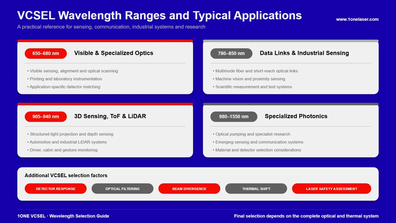
How Does Wavelength Affect the Application?
Wavelength influences detector response, filter selection, ambient-light interference, semiconductor material choice, optical loss, and safety assessment.
Wavelength Range | Common Application Direction | Main Design Considerations |
|---|---|---|
650–680 nm | Visible sensing, printing, specialized instruments | Visibility, detector response, material availability |
780–850 nm | Data links, industrial sensing, scientific systems | Fiber coupling, modulation speed, thermal drift |
850 nm | Multimode fiber, machine vision, proximity sensing | Link budget and detector sensitivity |
905–940 nm | 3D sensing, ToF, LiDAR, IR illumination | Peak power, ambient light, filtering, safety |
980 nm | Pumping, industrial and research systems | Thermal behavior, power density, packaging |
1300–1550 nm | Specialized communication and emerging sensing | Material system, detector choice, development cost |
A wavelength table is only a starting point.
Two projects using the same nominal wavelength may need very different pulse conditions, emitting areas, package formats, and thermal designs.
How to Select a VCSEL for a Project
A useful VCSEL inquiry should define the optical, electrical, mechanical, and environmental requirements.
1. Target Wavelength
Confirm detector response, optical filtering, transmission medium, and operating environment.
2. Operating Mode
Define whether the device will run in continuous-wave, modulated, short-pulse, or high-peak-current pulsed operation.
3. Optical Output
Separate average power, peak power, pulse energy, target irradiance, and total array output.
4. Emitter Configuration
Specify a single emitter, linear array, two-dimensional array, or custom pattern.
5. Beam Requirement
Provide divergence, spot size, uniformity, working distance, and field of view.
6. Thermal Conditions
Include ambient temperature, duty cycle, operating time, and available cooling space.
7. Package Format
Clarify whether the project needs bare die, submount, SMD package, optical module, or integrated assembly.
8. Quantity and Project Stage
State whether the requirement is for laboratory samples, prototypes, pilot production, or long-term OEM supply.
When Is a Custom VCSEL Solution Necessary?
A standard component is often the fastest path for initial evaluation.
Customization becomes more relevant when:
- A non-standard wavelength is required
- The emitter layout must match a specific optical system
- A custom VCSEL array is needed
- Peak pulsed output must be optimized
- A special divergence or beam profile is required
- Package dimensions are restricted
- Bare die or special bond-pad access is needed
- Thermal resistance must be reduced
- Custom testing and screening are required
- The project must move from samples into OEM production
Customization does not always mean redesigning the entire epitaxial or wafer structure.
In many projects, useful improvements can be achieved through array layout, submount design, packaging, driver conditions, diffusers, lenses, or application-specific testing.
How 1ONE VCSEL Supports Development
1ONE VCSEL supports R&D, testing, and OEM teams with VCSEL products, solutions, and deeper custom development.
A project discussion may include:
- Wavelength and power matching
- Single-emitter or array selection
- Continuous-wave and pulsed operation
- Bare-die and package options
- Beam and optical integration
- Thermal management
- Sample and prototype development
- Custom testing and screening
- OEM and ODM support
For special wavelengths, custom arrays, packaging, or complete optical modules, submit the project through Custom Development & ODM.
Frequently Asked Questions
What is the difference between a VCSEL and an edge-emitting laser?
A VCSEL emits through the top or bottom surface of the chip. An edge-emitting laser emits through the side. This affects cavity structure, beam geometry, wafer testing, packaging, and array integration.
Why is a VCSEL suitable for 3D sensing?
VCSELs can be arranged into compact arrays and support short-pulse or high-speed modulation. They also integrate well with diffusers and diffractive optical elements.
How should 850 nm and 940 nm VCSELs be compared?
The decision should consider detector response, ambient-light conditions, optical filtering, required range, power, and system-level safety.
Can a VCSEL be used in pulsed LiDAR?
Yes, but peak current, pulse width, repetition rate, duty cycle, junction temperature, and device lifetime must be verified.
Is every VCSEL eye-safe?
No. Laser safety depends on wavelength, output power, pulse conditions, beam diameter, divergence, exposure time, and the complete optical system.
Can small quantities be requested for evaluation?
Further Reading, Standards, and Technical References
The following resources provide additional background on VCSEL technology, laser product safety, U.S. regulatory considerations, and precision optical applications.
They are useful starting points for technical research and compliance planning, but they do not replace project-specific testing, laser safety assessment, product classification, or market-specific regulatory review.
- IEC 60825-1: Safety of Laser Products, Equipment Classification and Requirements IEC 60825-1 is an important international reference for laser product classification, measurement conditions, labeling, and manufacturer requirements. Engineering teams should confirm the applicable edition, amendments, and regional adoption for each project.
- FDA: Laser Products and Instruments This official FDA resource provides information about laser products, radiation-emitting product requirements, manufacturer responsibilities, and the U.S. regulatory framework. OEM teams should review the obligations that apply to their specific finished product.
- RP Photonics Encyclopedia: Vertical-Cavity Surface-Emitting Lasers This technical reference explains VCSEL structure, operating principles, beam characteristics, array configurations, and common application areas.
- K. Iga: Surface-Emitting Laser—Its Birth and Generation of New Optoelectronics Field This research paper reviews the development of surface-emitting lasers and their role in creating new optoelectronic technologies and applications.
- NIST Time and Frequency Division The National Institute of Standards and Technology provides research resources related to atomic clocks, frequency standards, precision timing, and measurement science. These topics offer useful context for VCSEL applications in compact atomic and precision optical systems.
Compliance note: A VCSEL die, a packaged laser component, and a finished laser product may carry different testing, classification, labeling, and documentation responsibilities. Final requirements depend on wavelength, output conditions, pulse mode, optical architecture, intended use, and target market.
From Device Parameters to a Working Application
The value of a VCSEL is not limited to vertical emission. It comes from combining fast modulation, scalable arrays, compact packaging, and semiconductor manufacturing in one optical platform.
A successful system, however, depends on more than the laser die.
The driver, receiver, optics, package, thermal path, and operating environment must work together.
The best selection process therefore starts with the application rather than the largest available power number.
Once wavelength, operating mode, target range, beam requirement, temperature range, package, and project stage are clear, the engineering team can determine whether a standard VCSEL is sufficient or whether the array, package, or complete optical module should be customized.